Why TSMC’s 2nm Chip Could Redefine Future Processors
Understanding the leap from 3nm to 2nm
When TSMC announced its roadmap toward a 2nm manufacturing process, the tech community took notice. The 2nm node represents more than a single‑nanometer shrink; it’s a shift in how transistors are arranged, how power is managed, and how much functionality can be packed onto a single silicon die. In practice, moving from 3nm to 2nm can shave a few percent off power consumption while boosting performance by a similar margin, but the real surprise lies in the architectural freedoms that become available.
At this scale, traditional planar transistors give way to gate‑all‑around (GAA) designs, where each nanowire is wrapped by the gate electrode. GAA offers tighter control over current flow, reducing leakage and allowing higher drive currents. For chip designers, that means tighter clocks without the thermal penalties that usually accompany speed gains.
Key technical challenges and how TSMC tackles them
Manufacturing at 2nm is not simply a matter of scaling down existing equipment. Lithography, the process that prints patterns onto wafers, must contend with wavelengths that approach the size of the features themselves. TSMC plans to rely heavily on extreme ultraviolet (EUV) tools equipped with high‑NA (numerical aperture) optics, a technology that only a handful of fabs currently possess.
- Pattern fidelity: As features shrink, any slight variation can cause a transistor to malfunction. Advanced process control, including real‑time metrology and AI‑assisted defect detection, helps keep yields acceptable.
- Materials science: Traditional silicon dioxide gate dielectrics struggle at these dimensions. Researchers are experimenting with high‑k metal oxides and even two‑dimensional materials like molybdenum disulfide to maintain insulating properties.
- Thermal management: Packing more transistors into the same area raises heat density. TSMC’s 2nm roadmap includes integrated micro‑fluidic cooling channels and novel packaging techniques that spread heat more efficiently.
These solutions are still in development, and early silicon runs may see lower yields than mature nodes. Yet the company’s incremental approach—first delivering a 2nm test chip, then scaling up to high‑volume production—mirrors how it handled the transition to 5nm and 3nm.
What the 2nm node could mean for consumer gadgets
For most end users, the benefits of a 2nm processor will manifest as longer battery life, smoother multitasking, and perhaps new capabilities that were previously out of reach due to power constraints. Imagine smartphones that can run advanced AI inference locally, without off‑loading to the cloud, while still lasting a full day on a single charge.
In laptops, the combination of higher performance per watt and thinner silicon could enable fan‑less designs that don’t compromise on speed. Even wearables—smart glasses, AR headsets, and health monitors—stand to gain from the reduced footprint, allowing more sensors and longer operation between charges.
Beyond portable devices, data centers could see a modest reduction in energy use per compute unit. While the percentage gain might appear small, the sheer scale of modern hyperscale facilities means any efficiency improvement translates into significant cost and carbon savings.
Industry ripple effects and competitive landscape
TSMC isn’t the only player eyeing sub‑3nm processes. Samsung and Intel have publicly discussed their own GAA‑based roadmaps, and each company is racing to claim the first high‑volume 2nm product. The winner will likely secure a strategic advantage in markets ranging from mobile SoCs to high‑performance computing accelerators.
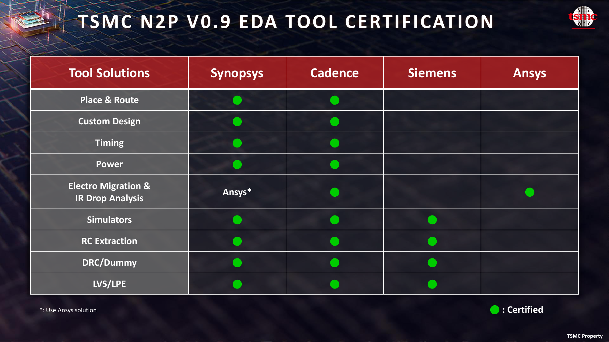
However, the race isn’t solely about raw transistor density. Ecosystem readiness—design tools, IP libraries, and software stacks—will determine how quickly the industry can translate a 2nm silicon wafer into a marketable chip. Foundries that provide robust design‑for‑manufacturability (DFM) support and flexible licensing models may attract more customers, even if their process node lags slightly behind the absolute smallest feature size.
For startups and smaller fabless companies, the cost of moving to 2nm could be prohibitive. That’s why many will likely continue to target 3nm or 4nm for the near term, reserving 2nm for flagship products where the performance premium justifies the expense.
Looking ahead: when can we expect 2nm devices?
TSMC’s public timeline suggests risk production of a 2nm test chip by 2025, with volume manufacturing slated for 2027. Assuming yields improve as anticipated, the first commercial devices—most likely high‑end smartphones or AI‑centric accelerators—could appear in 2028.
In the meantime, the industry will be watching closely for early silicon results. Real‑world measurements of power, performance, and thermal behavior will either confirm the optimistic projections or highlight unforeseen bottlenecks. Either outcome will shape the next generation of processor architecture, influencing everything from instruction set extensions to memory hierarchy designs.
Frequently Asked Questions
What is the main advantage of a 2nm chip over a 3nm one?
The primary benefit lies in higher transistor density, which enables better performance per watt and opens up new design possibilities such as more complex AI engines or additional security features within the same die area.
Will 2nm chips be more expensive for consumers?
Initially, yes. Early 2nm products will target premium segments where cost is less of a barrier. As the process matures and yields rise, prices are expected to converge with current high‑end 3nm offerings.
How does TSMC’s 2nm roadmap affect other semiconductor companies?
It raises the performance bar across the industry, prompting rivals to accelerate their own advanced‑node developments. This competitive pressure can lead to faster innovation and a broader range of options for device makers.
Is 2nm the ultimate limit for silicon?
Not necessarily. Physics suggests that continued scaling will eventually hit quantum mechanical limits, but researchers are already exploring alternatives like carbon‑based nanowires, silicon‑photonic integration, and three‑dimensional stacking that could extend Moore’s law beyond the traditional transistor node.